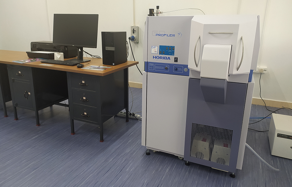
Feature
a) Quantitative elemental depth profile analysis from the first nanometer down to more than 150 microns
b) RF-Only generator is Class E standard and optimized for stability and crater shape allowing for real surface analysis
c) Source can be pulsed with synchronized acquisition for optimum results on fragile samples. The use of an RF source allows analysis of conventional and non conventional layers and materials
d) Simultaneous optic provides full spectral coverage from 110 to 800 nm, including deep UV access to analyze H, O, C, N and Cl
e) HORIBA original, ion-etched holographic gratings assure the highest light throughput and resolution for maximum light efficiency and sensitivity
f) Patented HDD detection provides speed and sensitivity in detection without compromise
Resolution/Specification:
a. Optional monochromator with Image mode and high Dynamic detection for full spectrum record and total flexibility
b. Pulsed RF Source for operation in RF and pulsed RF modes with auto-matching
c. Plasma Cleaning function built in
d. Patented UFS for Ultra-Fast Sputtering of polymeric and organic materials
e. Various anode diameters and accessories for odd shape samples
List of Facilities:
• Direct measurement of the depth as a function of time, with nanometric precision
(i) Depth profiling from few hundred nm to 150 microns
• Ultrafast elemental depth profile analysis of thin and thick layers, conducting or isolating, with high sensitivity to all elements
Application domains:
• Li batteries – positive and negative electrodes
• Nitriding – in-depth N and C measurements
• LED – depth resolution, process control
• Structured materials
• Hard disks – Uniformity check and repeatability
• Cationic exchange in glass
• Coatings on steel
• Polymer
• Hydrogen – H and D can be measured simultaneously
Sample Dimension and Structure:
• The samples size must be 3cm x 3cm or more
• The samples must be polished to mirror finish, free of oxide, grease and oil
• Smaller and thinner samples have lesser repeatability
• For non-conductive sample maintain the thickness 2mm or below