
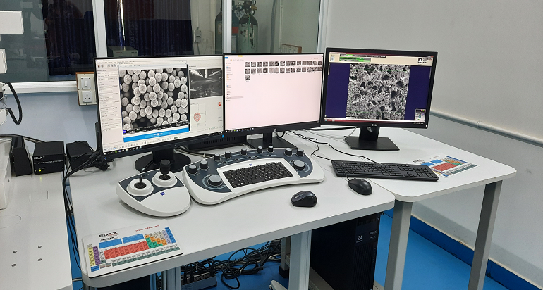

Facilities: High efficiency annular in-lens SE detector system, Energy selective back scattered detector for pure SE, pure BSE, and a mixture of SE+BSE signals, Everhart-Thornley detector, Six segment back scattered detector for Z contrast and crystal orientation, Quorum coater with gold, carbon and platinum source, PV 7600 SU A EDAX Octane super EDS System-SDD 70mm, EDAX Team EBSD system with Hikari plus, EDAX TEAM WDS-Texas HP stand alone system, aSTEM detector with tilt tomography holder with 0.6 nm @ 30 kV- Dark field (DF), Bright field (BF), Oriented dark field (ODF), annular dark field (ADF), High angular dark field (HAADF), 12 numbers of 3 mm TEM grids.
• Imaging –Grains, grain boundaries, their distribution in metals and alloys
• Dendrites, dendrite arms, their placings, coring in castings
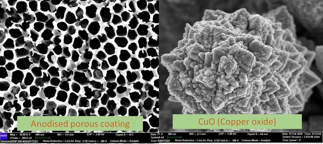
• Study of inclusions, slags, oxides, second phase investigations in metals and alloys
• Indications of deformations in deformed materials (rolling, forging, extrusions)
• Study of fractured surfaces (in failure analysis, forensic investigations)
• Study of composites (reinforcement distribution, interface reactions, etc.)
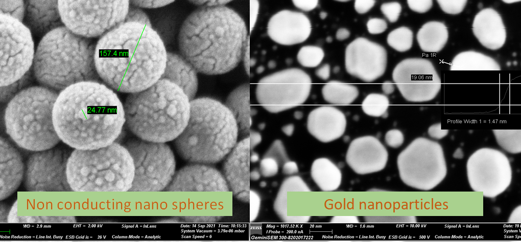
• Study of nanomaterials, biomaterials, energy materials, water purification media
• Study of ores and minerals, concrete materials (concrete mixes, cements, reinforcement steels), etc.
• Study of tribological systems (wear, erosion, abrasion)
• Textures in materials, pole figure mapping
• Composition mapping (point, line and area) using EDS and WDS
• Cored structures in nanomaterials
• Remaining life estimation of expensive and high risk structures
• Study of functional materials (nanoparticles, nanofibers, films, reflective and magnetic coatings, etc.)
Important Note:
1) Samples: Without proper code labelling will not be accepted.
2) Submission of samples: Submit samples immediately after slot confirmation. Stable samples must be submitted before 4:00 PM on Friday or the last working day before the experiment week. Applicants who submit samples early may be accommodated in vacant slots, with prior intimation. If samples are not submitted on time, the slot forms will be automatically cancelled.
3) Slot Date: Users whose sample required to be measured in particular date-period should inform operator post slot form submission, after assigning slot date request to postpone slot date will not be considered. Slot dates are tentative and subject to machine availability. In case of any preponement or postponement, applicants will be informed through email.
4) Slot Cancellation: User should inform the operator 3 working day before. Otherwise the slot will be cancelled & penalty will be imposed.
5) Slot Rescheduling: Postponement of slot dates is not permitted.
6) Slot Form: If Samples received via post without submitting signed form/ sample tagging, such samples will be discarded.
1. The samples should not should contain any acrylic/epoxy material.
2. Samples must be dry, free of moisture, free of oil and grease; Samples must be dessicated.
3. For Powder samples min. quantity 5mg, All analysis on non-mettalic and magnetic powder samples will be carried out below 3kV.
4. For solid (non-Degassing), size should be <= 1cm dimension per sample, height <= 1cm. if possible clean the sample with ethanol to remove oil and dust.
5. Since the current model of FESEM is not suitable for measuring biological samples (tissues, cells, etc). The CRF will not accept such samples.
6. Samples should not have any degassing species.
7. For Polymer and other non-conducting samples, analysis will be done @ < 4kV.
8. For Scratch/Tribo samples only 2 samples per slot is permitted.
| Details | Charge Basis | NITK# | Academia / R&D Institute* | Industry* |
|---|---|---|---|---|
| Only Imaging or Only EDS [max. 20 mins] | Per Sample | Rs. 720/- | Rs. 1200/- | Rs. 2400/- |
| Images + EDS [max. 30 mins] (10 images + 2 regions) | Per Sample | Rs. 1020/- | Rs. 1680/- | Rs. 3300/- |
| EDS Mapping or Line Scan (Per Scan) | Per Sample | Rs. 840/- | Rs. 1440/- | Rs. 2760/- |
| Images + Mapping or Line Scan (10 images + per scan) | Per Sample | Rs. 1140/- | Rs. 1920/- | Rs. 3660/- |
| Images + EDS + Mapping or Line Scan | Per Sample | Rs. 1320/- | Rs. 2160/- | Rs. 4200/- |
| Images + EDS + Mapping + Line Scan | Per Sample | Rs. 1500/- | Rs. 2400/- | Rs. 4800/- |
| Sputtering (Gold Coating) [Std. 100 sec] For non-conducting sample | Per Sample | Rs. 120/- | Rs. 180/- | Rs. 360/- |
| EBSD [Excluding sample preparation] | Per Hour | Rs. 1800/- | Rs. 3000/- | Rs. 4200/- |
| Details | Charge Basis | NITK# | Academia / R&D Institute* |
|---|---|---|---|
| Only Imaging or Only EDS [max. 20 mins] | Per Sample | Rs. 1080/- | Rs. 1800/- |
| Images + EDS [max. 30 mins] (10 images + 2 regions) | Per Sample | Rs. 1530/- | Rs. 2520/- |
| EDS Mapping or Line Scan (Per Scan) | Per Sample | Rs. 1260/- | Rs. 2160/- |
| Images + Mapping or Line Scan (10 images + per scan) | Per Sample | Rs. 1710/- | Rs. 2880/- |
| Images + EDS + Mapping or Line Scan | Per Sample | Rs. 1980/- | Rs. 3240/- |
| Images + EDS + Mapping + Line Scan | Per Sample | Rs. 2250/- | Rs. 3600/- |
| Sputtering (Gold Coating) [Std. 100 sec] For non-conducting sample | Per Sample | Rs. 180/- | Rs. 270/- |
| EBSD [Excluding sample preparation] | Per Hour | Rs. 2700/- | Rs. 4500/- |
#*Extra images and EDS will be charged Rs. 100/- per region.
#*Extra Mapping and Line Scan will be charged Rs. 250/- per scan.
*GST(18%) extra. Above charges are for providing raw data.